This blog skims through the technicalities of an ARM controller. Starting with the architecture, it proceeds to provide an overview of a simple assembly program. The nitty-gritty has been brushed aside and the incentive is to get the readers acclimated with how things work in an ARM processor.
Introduction
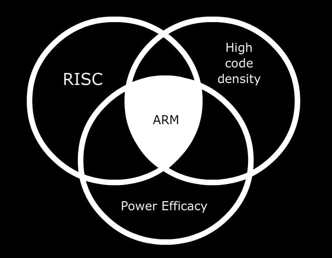
An ARM(Advanced RISC Machine) processor is one of a family of CPUs based on the RISC architecture. ARM as a company does not manufacture any processors. They design and sell them as a license to manufacturers such as Qualcomm, Texas Instruments, STMicroelectronics, etc. ARM processors do not abide by the native RISC architecture, instead, they make use of a mod compiling together the features of RISC, high code density, and power efficacy.
Reduced Instruction Set Computer aka RISC
There are two major computer architectures, RISC and CISC(Complex Instruction Set Computer). CISC lays greater complexity on the processor to interpret complex instructions, contrary to the RISC processors that work the compiler to interpret multiple lines of simpler codes.
RISC has four major design philosophies,
- Instructions: It makes use of simple fixed-length instructions. The programmers put together a number of these basic instructions to achieve complicated operations.
- Pipelines:
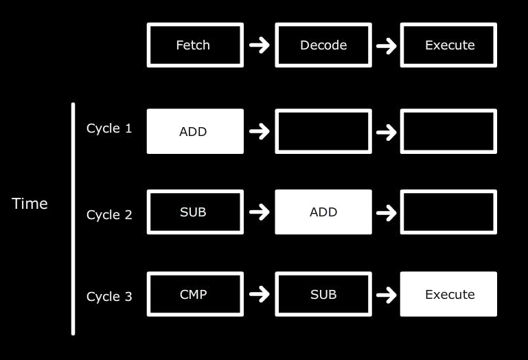 Shown above is a simple three-stage pipeline architecture. Some implementations in cores like Cortex-A used in smartphones have as many as 15 stages. As the pipeline length increases, the amount of work done per cycle decreases, hence allowing the processor to attain higher operating frequencies. This in turn increases the performance and system latency.
 - RISC processors have a large number of registers. This is the local memory closest to the processor. Any operation on data in the computer memory is performed after loading it into the registers.
- Load-Store Architecture: External memory accesses are expensive in terms of performance. To mitigate this, the processor first loads the data items into the registers and then performs operations on them. As this separates the memory accesses from data processing, data items can be reused as required when they are stored in the register.
ARM Core Data Flow Model
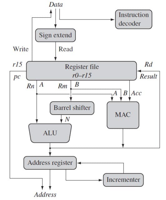
(i) The instruction decoder translates instructions before they are executed. Each instruction executed belongs to a particular instruction set.
(ii) The register file is a storage bank made up of 32-bit registers. Most instructions treat the registers as holding signed/unsigned 32-bit values. ARM instructions typically have two source registers, Rn and Rm, and a single result or destination register, Rd.
(iii) The ALU(Arithmetic Logic Unit) and MAC(Multiply-accumulate unit) take values from the register, Rn and Rm, perform the required operation, and use data processing instructions to write the result to the destination register, Rd. For load and store instructions, the ALU is used to generate an address to be held in the address register.
(iv) Barrel shifters are small circuits that are designed to shift/rotate data.
(v) The incrementer updates the address registers before the core reads/writes to the next register from a sequential memory location.
Banked Registers
The architecture of an ARM Cortex-M is quite different from other ARM processors. The Cortex-M has,
- 17 General Purpose Registers
- 1 Status Register
- 3 Interrupt Mask Registers
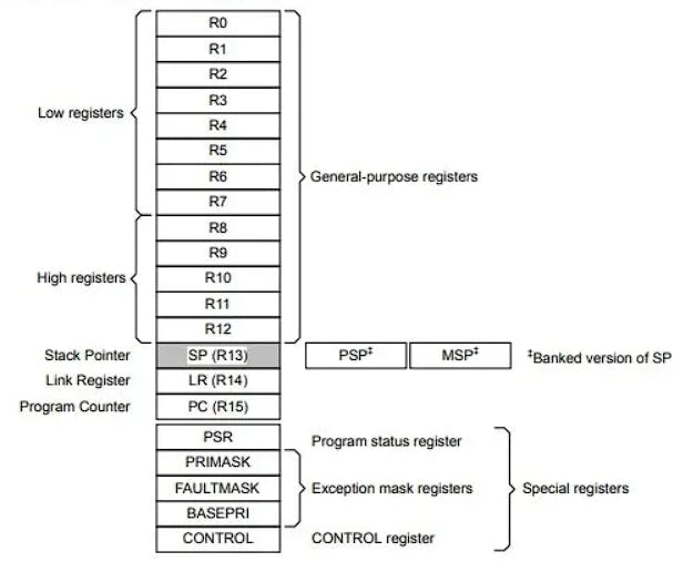
- The General Purpose registers contain data and addresses.
- Stack pointer(R13) points to the top element of the stack.
- Link Register(R14) is used to hold the return address of functions.
- The Program counter(R15) holds the address of the instruction being fetched.
That's enough theory for now, and we'll have a look at all of these on the fly as we work on some assembly programming. The next section provides a brief overview of assembly programming and its syntax. Again, there are different kinds of instruction sets, and talking about all of them will only make this blog way more boring than it has already been.
Introduction to Assembly Programming
Since this is the first part of the series, let's keep things a little light and glance through an assembly snippet that adds two numbers and moves the result to a register.
ARM instructions are representations of binary codes. For instance, the instructions, ADD internally could represent a 4-bit code like 1001. Analogous to this, ARM instructions are 32 bits wide and operate on 32-bit data.
; This is a simple assembly program that adds two numbers

        AREA SimpleProject, CODE, READONLY   ;Assembling a new readonly code block
        ENTRY                                ;This is the program's entry
        EXPORT __main                        ;Export __main

__main

        MOV R1, #0x01        ;Store hexadecimal value 0x01 in R1
        MOV R2, #0x01        ;Store hexadecimal value 0x01 in R2
        ADD R4, R1, R2       ;ADD R1 and R4 and store the result R4

STOP     B STOP                ;STOP
         END                   ;END
AREA SimpleProject, CODE, READONLY ;Assembling a new readonly code block
- The AREA instruction here assembles a new read-only code section called SimpleProject.
- ENTRY denotes the start of the program.
- __main is a label that is exported to the startup file(A pre-built program that gets executed on the microcontroller).
- The instructions under __main label get executed.
Let's have a look at how the registers look after executing the program.
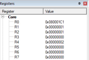
The hexadecimal value, 0x01 is moved to the registers R1 and R2. The instruction ADD adds the values stored in these registers and stores the sum(0x02) in R4.
Conclusion
This blog is a starter to this series and a lot of it may have sounded too abstract, but I'm quite sure it'll get better with the sequels.
References:
- https://theorycircuit.com/wp-content/uploads/2017/03/arm-core-data-flow.jpg
- https://i0.wp.com/microcontrollerslab.com/wp-content/uploads/2020/07/ARM-Cortex-M4-microcontroller-Registers.jpg?w=800&ssl=1
- https://www.udemy.com/course/arm-assembly-language-from-ground-uptm-2/
- B. Shantha Kumar Naik, ARM CONTROLLER, 1st rev, Bengaluru, Sapna Book House (P) Ltd; 2017.

